


How graphene skip silicon limits to build nanoelectronic

How graphene skip silicon limits to build nanoelectronic
Atomically thin transistors and circuits made of graphene and molybdenum disulfide (molybdenite) can now be chemically assembled on a large scale, researchers say. Previous attempts to build circuits from 2-D materials involved placing materials precisely instead of growing them where they’re needed.
Researchers hope such atomically-thin devices will allow Moore’s Law to continue once it becomes impossible to make further progress using silicon. “A big drive for nanotechnology has been the search for new materials to replace silicon to meet Moore’s law,” says study senior author Xiang Zhang, a materials scientist at the University of California Berkeley.
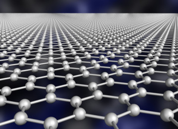
Research into next-generation electronics has recently explored atomically thin materials such as graphene or molybdenite. Graphene is an excellent conductor, making it ideal for use in wiring and interconnections. However, graphene lacks an electronic band gap, meaning that it cannot easily be used in transistors. In contrast, molybdenite, or molybdenum disulfide (MoS2), has an electronic band gap.
Manufacturing atomically thin electronics has proven challenging because assembling precise structures from both conductive and semiconducting materials has proven extremely difficult. Now scientists have created transistors and circuits each woven from both conductive graphene and semiconducting molybdenite.
The previous research sought to physically assemble atomically thin electronics by placing different materials together. Instead, this new work chemically grows these electronics on a large scale.

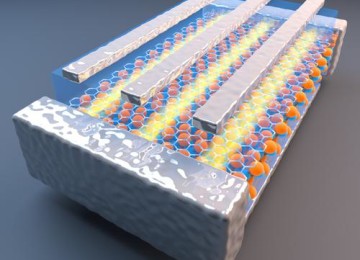
How graphene joins with molybdenite (MoS2) to build electronics
First, the researchers transferred graphene onto silica and used plasma to etch patterns of channels onto it. They next used Chemical Vapor Deposition (CVD) to grow molybdenite around the edges of each channel until it completely filled the channels. The molybdenite strips overlapped about 100 to 200 nanometers on top of the graphene.
The resulting transistors had high electron mobilities comparable to those of similar devices assembled physically. The scientists also assembled an atomically thin logic circuit specifically, an inverter, or NOT gate. This circuit demonstrated a voltage gain of up to 70, a key quality for inverters.
“We used the transistors to form an inverter and demonstrate that logic is possible with our devices,” says study lead author Mervin Zhao, a materials scientist at the University of California Berkeley. “This is a platform for making more complex circuits, and therefore computers, using completely 2-D materials.”
Zhao does caution that in this preliminary work, the molybdenite channels are about 2 micrometers wide. “If this technology were truly be used as a silicon replacement, we need extremely thin transistor channels,” Zhao says. It remains uncertain what molybdenite performance will be like when transistor channels get very narrow, he says.
The scientists detailed their findings online in the journal Nature Nanotechnology. “We have filed a provisional patent for this work,” Zhao adds.