


Diamond help produce high-quality graphene with low cost
Diamond help produce high-quality graphene with low cost
Argonne Labs and UC Riverside have developed a method to grow graphene that contains relatively few impurities and costs less to make, in a shorter time and at lower temperatures compared to the processes widely used to make graphene today.
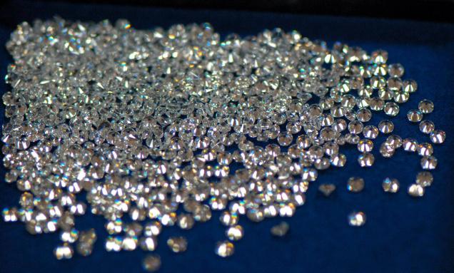
The new technology taps ultra-nanocrystalline diamond (UNCD), a synthetic type of diamond that Argonne researchers have pioneered through years of research. UNCD serves as a physical substrate, or surface on which the graphene grows, and the source for the carbon atoms that make up a rapidly produced graphene sheet.
The degradation of intrinsic properties of graphene during the transfer process constitutes a major challenge in graphene device fabrication, stimulating the need for direct growth of graphene on dielectric substrates. Previous attempts of a metal-induced transformation of diamond and silicon carbide into graphene suffers from metal contamination and inability to scale graphene growth over the large area. Here, we introduce a direct approach to transforming polycrystalline diamond into high-quality graphene layers on the wafer scale (4 inches in diameter) using a rapid thermal annealing process facilitated by a nickel, Ni thin film catalyst on top. We show that the process can be tuned to grow single or multilayer graphene with good electronic properties. Molecular dynamics simulations elucidate the mechanism of graphene growth on the polycrystalline diamond. In addition, we demonstrate the lateral growth of free-standing graphene over micron-sized pre-fabricated holes, opening exciting opportunities for future graphene/diamond-based electronics.
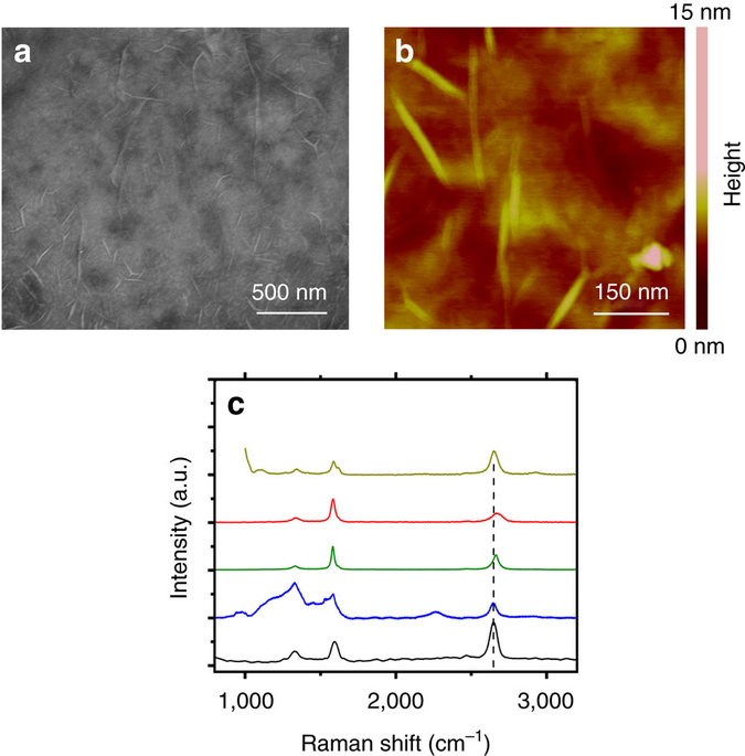
“When I first looked at the [scanning electron micrograph] and saw this nice uniform, very complete layer, it was amazing,” said Diana Berman, the first author of the study and former postdoctoral research associate who worked with Sumant and is now an Assistant Professor at the University of North Texas. “I’d been dealing with all these different techniques of growing graphene, and you never see such a uniform, smooth surface.”
Current graphene fabrication protocols introduce impurities during the etching process itself, which involves adding acid and extra polymers, and when they are transferred to a different substrate for use in electronics.
“The impurities introduced during this etching and the transferring step negatively affect the electronic properties of the graphene,” Sumant said. “So you do not get the intrinsic properties of the graphene when you actually do this transfer.”
Graphene on diamond appear in nanoscale
The team found that the single-layer, single-domain graphene can be grown over micron-size holes laterally, making them completely free-standing (that is, detached from the underlying substrate). This makes it possible to exploit the intrinsic properties of graphene by fabricating devices directly over free-standing graphene.
The new process is also much more cost-effective than conventional methods based on using silicon carbide as a substrate. Sumant says that the 3- to 4-inch silicon carbide wafers used in these types of growth methods cost about $1,200, while UNCD films on silicon wafers cost less than $500 to make.
The diamond method also takes less than a minute to grow a sheet of graphene, where the conventional method takes on the order of hours
“The proven predictive power of our simulations places us in a position of advantage to enable rapid discovery of new catalytic alloys that mediate growth of high-quality graphene on dielectrics and move away on their own when the growth is completed,” added Narayanan.
In addition to the utility in making minimally defective, application-ready graphene for things like low-frequency vibration sensors, radio frequency transistors and better electrodes for water purification, Berman and Sumant say that the Argonne team has already secured three patents arising from their new graphene growth method.
The researchers have already struck a collaboration with Swedish Institute of Space Physics involving the European Space Agency for their Jupiter Icy Moons Explorer (JUICE) program to develop graphene-coated probes that may help exploratory vehicles sense the properties of plasma surrounding the moons of Jupiter.
Closer to home, the team has also crafted diamond and graphene needles for researchers at North Carolina University to use in biosensing applications.
The Argonne researchers are now fine-tuning the process – tweaking the temperature used to catalyze the reaction and adjusting the thickness of the diamond substrate and the composition of the metal film that facilitates the graphene growth – to both optimize the reaction and to better study physics at the graphene-diamond interface.
“We’re trying to tune this more carefully to have a better understanding of which conditions lead to what quality of graphene we’re seeing,” Berman said.