


Graphene coating improves electron microscopy images
Graphene coating improves electron microscopy images
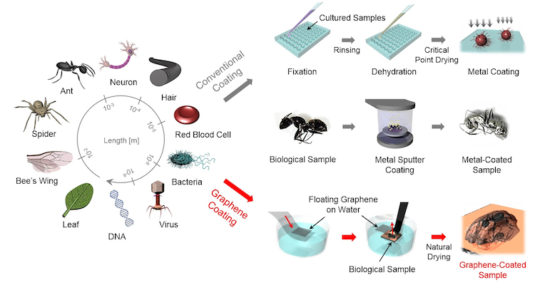
Researchers in Korea and the UK have discovered that a graphene coating on biological samples helps dissipate the charge build-up that normally occurs on the surface of these samples during non-destructive electron microscopy imaging. Such a charge build-up is usually a big problem in this context and prevents high-resolution images from being obtained.
Gold or platinum coatings are usually used to prevent samples from charging up in an electron microscope, but these coatings mean that researchers cannot obtain high-resolution images of the samples or perform further quantitative and qualitative chemical analyses with techniques such as energy dispersive spectroscopy (EDS).
Now, a team led by Byung Hee Hong of Seoul National University and Konstantin Novoselov of the University of Manchester have discovered that an atomically thin coating of carbon (graphene) on biological samples dissipates this charge accumulation on the non-conducting surfaces of biological samples.
Graphene membrane provides conducting channels:
This is possible thanks to the high electrical conductivity of graphene, says team member Diby Kim. “As soon as excessive charges appear on the sample surfaces, the graphene membrane provides conducting channels for these charges to disappear quickly and so allows us to obtain high-resolution EM images. What is more, the high thermal conductivity of graphene allows it to dissipate excess heat produced by the high-energy electrons in the microscope, so preventing thermal damage or deformation of biological specimens as well.”
Thanks to the fact that graphene is highly transparent to an electron beam, the electrons easily pass through the graphene and penetrate deep into the sample, he adds. These electrons excite various atoms inside the sample and eventually produce characteristic X-rays, which can then escape very easily from the sample through the graphene membrane and to an EDS detector, for example. In contrast, electrons are blocked from entering metal-coated biological samples and any X-rays produced inside the sample cannot easily escape either because of the large electron-scattering cross-section of the metal coatings.
Graphene vs metal coating
Fine surface features revealed:
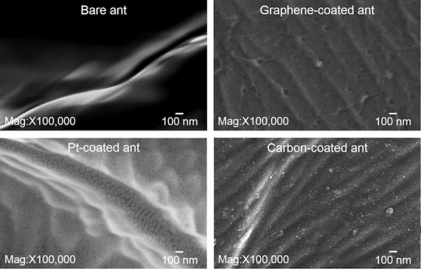
The researchers tested out their technique on ants that they had coated either with a thin metal film or a graphene membrane. They found that they were not able to observe the fine surface features of the insects because of the large surface roughness of the metal film. With the graphene membrane, this problem did not exist.
“More interestingly, we found that the graphene is suitable for encapsulating macromolecules (DNAs or proteins, for example) in a liquid environment and that it was stable in a vacuum,” Kim tells nanotechweb.org. “This allows us to obtain in situ and real-time EM images of biological processes occurring in these molecules, something that cannot easily be done in EM samples prepared using conventional methods, which only work in the high vacuum.”
Unveiling secrets of the biological world never seen before:
Bo Chen of the University of Central Florida, who was not involved in this work, says that Novoselov, Hong, and colleagues have “conducted an in-depth study of the important advantages of adopting graphene as the support and coating material in electron microscopy characterizations of biological samples that vary in size from nanometres to microns. The unique combination of mechanical strength and superb conductivity of graphene enables non-invasive and high-resolution imaging of these delicate samples that cannot be achieved otherwise. Coupled with the recent advances in direct electron detection chips, it is very likely that electron microscopy will unveil secrets of the biological world that we have never seen before.”
The researchers, reporting their work in 2D Materials doi:10.1088/2053-1583/3/4/045004, say that their technique provides them with a new way to explore biological phenomena. “For example, we are planning to observe how biological objects encapsulated with graphene self-assemble in liquids,” says Kim. “Attempts to do this with other techniques, such as cryogenic transmission electron microscopy (TEM) and topographic imaging by atomic force microscopy (AFM) have proved unsuccessful for when it comes to observing these real-time processes, so we believe that our technique will help shed new light on these.”