Graphene in plasmonics could detect dangerous materials

Graphene in plasmonics could detect dangerous materials
Physicists from the Moscow Institute of Physics and Technology (MIPT) have found that the two-dimensional form of carbon, known as graphene, might be the ideal material for manufacturing plasmonic devices capable of detecting explosive materials, toxic chemicals, and other organic compounds based on a single molecule, says an article published in Physical Review B.
Scientists have long been fascinated by the potential applications of a quasiparticle called the plasmon, a quantum of plasma oscillations. In the case of a solid body, plasmons are the oscillations of free electrons. Of special interest are the effects arising from the surface interactions of electromagnetic waves with plasmons – usually in the context of metals or semimetals, as they have a higher free electron density.
Harnessing these effects could bring about a breakthrough in high-accuracy electronics and optics. One possibility opened up by plasmonic effects is the subwavelength light focusing, which increases the sensitivity of plasmonic devices to a point where they can distinguish a single molecule.
Such measurements are beyond what any conventional (classical) optical devices can achieve. Unfortunately, plasmons in metals tend to lose energy quickly due to resistance, and for this reason, they are not self-sustained, i.e. they need continuous excitation. Scientists are trying to tackle this issue by using composite materials with predefined microstructure, including graphene.
Graphene is an allotrope of carbon in the form of a two-dimensional crystal. It can be visualized as a one-atom-thick honeycomb lattice made of carbon atoms. Two MIPT graduates, Andre Geim and Konstantin Novoselov, were the first to isolate graphene, which won them a Nobel Prize in Physics. Graphene is a semiconductor with extremely high charge carrier mobility. Its electrical conductivity is also exceptionally high, which makes graphene-based transistors possible.
Although plasmonic devices have seemed an exciting prospect to pursue from the start, to take advantage of them, it was first necessary to find out whether the technology behind them was feasible. To do this, scientists had to find a numerical solution to the relevant quantum-mechanical equations.
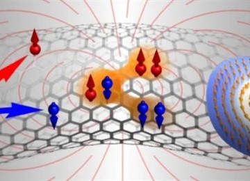
This was accomplished by a team of researchers at the Laboratory of Nanostructure Spectroscopy headed by Prof. Yurii Lozovik: they formulated and solved the necessary equation. Their research has led them to develop a quantum model that predicts plasmonic behavior in graphene. As a result, the scientists described the operation of a surface-plasmon-emitting diode (SPED) and the nanoplasmonic counterpart of the laser – known as the spaser – whose construction involves a graphene layer.
A spaser could be described as a device similar to a laser and operating on the same basic principle. However, to produce radiation, it relies on optical transitions in the gain medium, and the particles emitted are surface plasmons, as opposed to photons produced by a laser. A SPED is different from a spaser in that it is an incoherent source of surface plasmons. It also requires considerably lower pump power. Both devices would operate within the infrared region of the spectrum, which is useful for studying biological molecules.
‘The graphene spaser could be used to design compact spectral measurement devices capable of detecting even a single molecule of a substance, which is essential for many potential applications.
‘Such sensors could detect organic molecules based on their characteristic vibrational transitions (‘fingerprints’), as the light emitted/absorbed falls into the medium infrared region, which is exactly where the graphene-based spaser operates,’ says Alexander Dorofeenko, one of the authors of the study.

