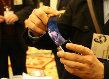


Graphene semiconductors combined to make optical techniques probe
Graphene Semiconductors Combined to make Optical Techniques Probe
When graphene is to beat out normal semiconductor tech in the race to become the foundation the next generation of integrated circuits, determining its band-gap potentials is crucial. That fundamental information had not been available until researchers at the National Institutes of Standards and Technology (NIST) yoked two optical measurement techniques into a non-destructive method that provides the first complete picture of a Graphene Insulator Semiconductor (GIS) device in photoemission spectroscopy. From the flat band voltage and Dirac voltage, negative extrinsic charge present on the graphene surface. Also, researchers extract the graphene work function to be 4.56 eV, in excellent agreement with theoretical and experimental values in literature. Electron and hole injection from heavily doped p-type silicon (Si) is both observed. The barrier height from the top of the valence band of Si to the bottom of the conduction band of silicon dioxide (SiO2) is found to be 4.3 eV. The small optical absorption in graphene makes it a good transparent contact to enable the direct observation of hole injection from Si to graphene. The barrier height for holes escaping from the bottom of Si conduction band to the top of SiO2valence band is found to be 4.6 eV.
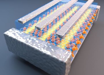
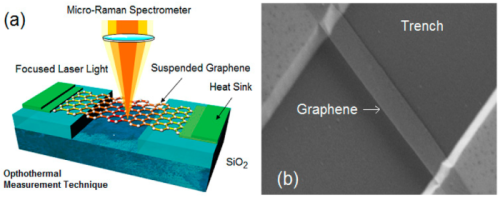
Illustration Graphene Semiconductors and how Graphene Insulator Semiconductor (GIS) manufacturing
Researchers at the NIST Physical Measurement Lab combined two long-established spectroscopic methods—internal photoemission (IPE) spectroscopy and spectroscopic ellipsometry. Both exploit the essential transparency of the graphene monolayer to flesh out the picture of electron transport in a graphene/silicon dioxide/p-type silicon sandwich. Understanding and controlling the band-gap structure is vital: poorly structured band offsets could result in current leakage and even component failure. Previous approaches to measuring band structure, such as cross-sectioning the device, destroyed the test component, making iterative experiments impossible and, indeed, sometimes altering the very characteristics they were trying to measure.
Internal photoemission spectroscopy correlates the energy and wavelength of photons striking a surface with the energy of emitted electrons. Ellipsometry measures change in the polarization of reflected light, and can reveal energy-band transitions on the surface. Both techniques have their foundations in the 1880s but have only recently been combined. As an NIST summary describes it, internal photoemission shows the bands’ offset and alignment, and ellipsometry facilitated calculation of the band gaps. Together, the two techniques allowed Nguyen and colleagues to completely characterize the material’s electrical structure.
“IPE technique has been around for a long time to characterize electronic interfacial properties, band offset at the solid/solid interface in particular. Traditionally it has been used to study MOS interfaces,” says Nguyen. “Only recently we have advanced the technique by combining it with ellipsometry and special test structure design to enable successful characterization of more complicated structures such as certain semiconductor heterojunctions (metal/oxide/heterojunction) used in TFET [tunneling field effect transistors].”
The NIST researchers plotted photoemission output for a variety of gate voltages and incident photon energies across the graphene-insulator-semiconductor interface. They found the gate voltage at which the photocurrent dropped to zero (the flatband voltage), which provided a foundation for calculating the rest of the band structure. The researchers thus derived the work function (the energy needed to lift an electron from the valence band into the conduction band), barrier heights, band widths, and other parameters.
“Most strikingly,” the NIST team wrote in their Applied Physics Letters description of the work, “the measurements of all these quantities…allows us to accurately depict the band alignment in the graphene-SiO2-Si structure.” Moreover, they said, “graphene can be used as an ideal transparent contact for IPE measurements to enable[e] the observation of hole injection. We believe that the key band structure reported here will pave the way for future studies on electrical and optical devices utilizing a GIG (or GIS) configuration.”