


Graphene transistor increases processors speed and uses power less
Graphene transistor increases processors speed and uses power less
Russian scientists from the Moscow Institute of Physics and Technology (MIPT), the Institute of Physics and Technology RAS, and Tohoku University in Japan, proposed a new design for a tunnel transistor based on bilayer graphene, and using modelling, they proved that this material is an ideal platform for low-voltage electronics.
In a continuous search for the energy-efficient electronic switches, a great attention is focused on tunnel field-effect transistors (TFETs) demonstrating an abrupt dependence of the source-drain current on the gate voltage. Scientists have developed a new type of graphene transistor and using modelling they have demonstrated that it has ultra low power consumption compared with other similar transistor devices. Reducing power consumption enables the clock speed of processors to be increased, according to calculations, to as high as two orders of magnitude, since the electronic components heat up less it’s good to make processors better in performance and save power.
Building transistors that are capable of switching at low voltages (less than 0.5 volts) is one of the greatest challenges of modern electronics.
Tunnel FETs (TFETs) with interband tunneling are among the principal candidates to meet this demand. The low-voltage switching in TFETs occurs due to a sharp dependence of the tunnel current on the conduction-valence band overlap in a gate-controlled p-i or p-n junction once there is no band overlap, there is no tunnel current. This fact, alongside with the smallness of thermionic leakage current and efficient modulation of the barrier transparency by the gate voltage, results in the subthreshold slope of the TFET characteristics surpassing the thermionic limit of (60 mV/dec).
So Tunnel transistors are the most promising candidates to solve this problem. Unlike in conventional transistors, where electrons “jump” through the energy barrier, in tunnel transistors the electrons “filter” through the barrier due to the quantum tunneling effect. However, in most semiconductors the tunneling current is very small and this prevents transistors that are based on these materials from being used in real circuits.
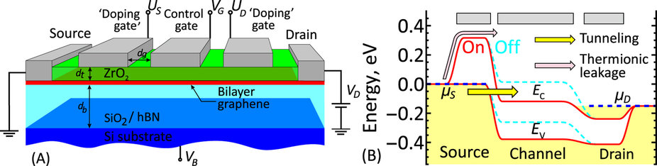
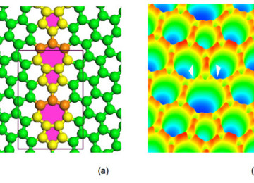
Layout of the proposed graphene bilayer TFET with electrically defined source and drain regions (B) Band diagram of graphene bilayer TFET for the optimal biasing conditions
Graphene, which was created by MIPT alumni Sir Andre Geim and Sir Konstantin Novoselov, is a sheet of carbon that is one atom thick. As it has only two dimensions, the properties of graphene, including its electronic properties, are radically different to three-dimensional carbon graphite.
“Bilayer graphene is two sheets of graphene that are attached to one another with ordinary covalent bonds. It is as easy to make as monolayer graphene, but due to the unique structure of its electronic bands, it is a highly promising material for low-voltage tunneling switches,” says Svintsov.
Bands of bilayer graphene, i.e. the allowed energy levels of an electron at a given value of momentum, are in the shape of a “Mexican hat”. It turns out that the density of electrons that can occupy spaces close to the edges of the “Mexican hat” tends to infinity – this is called a van Hove singularity. With the application of even a very small voltage to the gate of a transistor, a huge number of electrons at the edges of the “Mexican hat” begin to tunnel at the same time. This causes a sharp change in current from the application of a small voltage, and this low voltage is the reason for the record low power consumption.
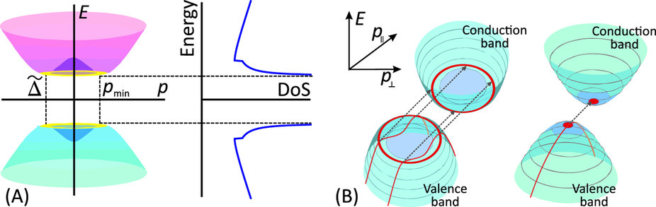
Electron spectrum E(p) in graphene bilayer under transverse electric field and law leads to the square-root singularities
In their paper, the researchers point out that until recently, van Hove singularity was barely noticeable in bilayer graphene – the edges of the “Mexican hat” were indistinct due to the low quality of the samples. Modern graphene samples on hexagonal boron nitride (hBN) substrates are of much better quality, and pronounced van Hove singularities have been experimentally confirmed in the samples using scanning probe microscopy and infrared absorption spectroscopy.
An important feature of the proposed transistor is the use of “electrical doping” (the field effect) to create a tunneling p-n junction. The complex process of chemical doping, which is required when building transistors on three-dimensional semiconductors, is not needed (and can even be damaging) for bilayer graphene. In electrical doping, additional electrons (or holes) occur in graphene due to the attraction towards closely positioned doping gates.
Under optimum conditions, a graphene transistor can change the current in a circuit ten thousand times with a gate voltage swing of only 150 millivolts.
“This means that the transistor requires less energy for switching, chips will require less energy, less heat will be generated, less powerful cooling systems will be needed, and clock speeds can be increased without the worry that the excess heat will destroy the chip,” says Svintsov.