


Laser-induced graphene creates super nano-defects
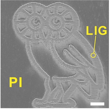
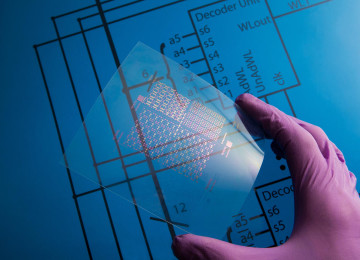
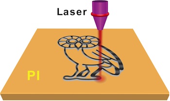
Rice University Owl was produced by burning a graphene foam pattern into a flexible polyimide sheet with a laser
Since few years researchers at Rice University have created flexible, patterned sheets of multilayer graphene from a cheap polymer by burning it with a computer-controlled laser. The process works in air at room temperature and eliminates the need for hot furnaces and controlled environments, and it makes graphene that may be suitable for electronics or energy storage.
Under a microscope, what the researchers call laser-induced graphene (LIG) doesn’t look like a perfect chicken wire-like grid of atoms. Instead, it’s a jumble of interconnected graphene flakes with five-, six- and seven-atom rings. The paired five- and seven-atom rings are considered defects – but in this case, they’re not. They’re features.
The material can be made in detailed patterns. For show-and-tell, the Rice team patterned millimeter-sized LIG Owls (the school’s mascot), and for practical testing, they fabricated microscale supercapacitors with LIG electrodes in one-step scribing.
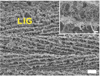
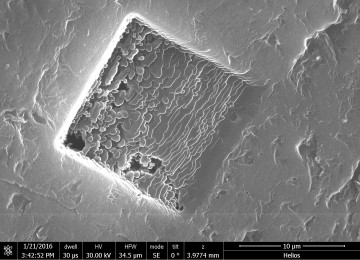
A scanning electron microscope shows a close-up of laser-induced graphene foam produced by researchers at Rice University. The scale bar for the main image is 10 microns
The one-step process is scalable, said Tour, who suggested it could allow for rapid roll-to-roll manufacture of nanoscale electronics.
“This will be good for items people can relate to clothing and wearable electronics like smartwatches that configure to your smartphone,” he said.
This top-down approach to making graphene is quite different from previous works by Tour’s lab, which pioneered the smLaser-induced graphene create super nano-defects-scale manufacture of the atom-thick material from common carbon sources, even Girl Scout cookies, and learned to split multiwalled nanotubes into useful graphene nanoribbons.
But as in the previous work, the base material for LIG is inexpensive. “You buy polyimide flexible plastic sheets in huge rolls, called Kapton, and the process is done entirely in the air with a rapid writing process. That sets it up for a very scalable, industrial process,” Tour said.
The product is not a two-dimensional slice of graphene but a porous foam of interconnected flakes about 20 microns thick. The laser doesn’t cut all the way through, so the foam remains attached to a manageable, insulating, flexible plastic base.
The laser removes nearly everything but carbon from a 20-micron layer, leaving behind porous graphene foam that may be suitable for electronics or energy storage.
The process only works with a particular polymer. The researchers led by Jian Lin, a former postdoctoral research in the Tour Group and now an assistant professor at the University of Missouri, tried 15 different polymers and found only two could be converted to LIG. Of those, polyimide was clearly the best.
Miguel José Yacaman, chairman of the Department of Physics at the University of Texas at San Antonio, contributed his expertise in transmission electron microscope imaging to confirm the existence of so many defects.
“We have what is called aberration-corrected microscopy, which allows us to see the defects,” Yacaman said. “The resolution is below 1 angstrom, basically 70 picometers (trillionths of a meter), and that’s what you need to really look at single atoms.”
Tour’s lab used the machine shop lasers at Rice’s Oshman Engineering Design Kitchen to create their robust micro-supercapacitors. The best results showed capacitance of more than 4 millifarads per square centimeter and power density of about 9 milliwatts per square centimeter, comparable to other carbon-based micro-supercapacitors, and negligible degradation after as many as 9,000 charge/discharge cycles. This capacitance is sufficient for inexpensive wearable electronic devices, and Tour said his group continues to make improvements.
He said the lab didn’t start out looking for LIG. “Everything converged. Nature can be a hard taskmaster, but once in a while, she gives you something much better than what you had asked for. Or expected.”