


New patent for a 3D printer that can print a graphene-based OLED
3D printer that can print a graphene-based OLED layers
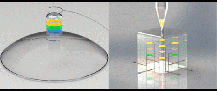
An American company called Graphene 3D Lab has announced filing a provisional patent for a process of 3D printing an OLED light source that immediately functions when printed, with a graphene coated transparent conductor window. This unique structure is the product of an innovative multi-functional 3D Printer, which can make thin films as well as 3D structures, Graphene 3D Lab, Inc was spun-off Graphene Labs in November 2013 to focus on the development of high-performance graphene-enhanced materials for 3D printing.
The printer patent relates to a technology that should lead the industry in multiple deposition techniques, robotic manipulator, laser and UV curing capabilities. G3L considers the new IP a dramatic leap forward, offering the ability to 3D print with multiple functional materials at the same time, including the ability to 3D print a working light. This printer was reportedly designed to maximize the attributes of the functional materials that the company already developed, and plans to introduce in the future to the market.
The printer will not be available immediately for pre-order. The company is currently evaluating contract manufacturing and partnership opportunities to support commercialization of the printer.
3D printer can print OLED display
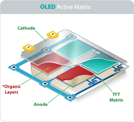
This big step come after a lot of steps started in the Fraunhofer FEP is coordinating the GLADIATOR project and acts as an end-user of the graphene electrode. Scientists examine the integration of graphene and compare it to the reference material ITO. The sophisticated material properties of graphene must be maintained during the integration in organic devices. To this end, several methods for cleaning and structuring the graphene must be modified. In addition, the processes for different target substrates such as glass or flexible foil must be adapted and optimized. The first hurdles have been overcome thanks to a close cooperation between the consortium partners and the first defect-free OLEDs on transparent graphene electrodes have been realized on small areas. The target of the next one and a half years is to successfully illuminate large area OLEDs. The GLADIATOR project will run until April 2017. By this time, several types of OLED will have been made using graphene electrodes: a white OLED with an area of about 42 (cm)2 to demonstrate the high conductivity, and a fully-flexible, transparent OLED with an area of 3 (cm)2 to confirm the mechanical reliability. Source and top image: Fraunhofer FEP Learn more at the next leading event on the topic: Printed Electronics Europe 2016 on 27 – 28 Apr 2016 in Berlin, Germany hosted by IDTechEx.
The Fraunhofer Institute for Organic Electronics, Electron Beam and Plasma Technology FEP will show for the first time the organic light emitting diodes (OLEDs) on graphene. These OLEDs are an interim result from the project GLADIATOR funded by the European Commission. Until now transparent electrode materials for OLEDs have mainly consisted of indium tin oxide (ITO), which is expected to become economically challenging for the industry due to the shrinking abundance of indium. Therefore, scientists are intensively looking for alternatives. One promising candidate is graphene, whose application fields are more closely investigated in the project GLADIATOR (“Graphene Layers: Production, Characterization and Integration”). The project GLADIATOR, which is funded by the European Commission, has reached its midterm and has already achieved some successes. The aim of the project is the cost-effective production of high-quality graphene at a large area, which can then be used for numerous electrode applications. The usability of such applications will be demonstrated at the Fraunhofer FEP by integrating this graphene in OLEDs.