


New tech makes bilayer graphene has high quality
New tech makes bilayer graphene has high quality
American researchers at the University of Texas at Austin, Columbia University, and the IBS Center for Multidimensional Carbon Materials at the Ulsan National Institute of Science and Technology, Korea and China has developed a new way to make bilayer graphene that is higher in quality than that produced by any other known process, by “Bernal-stacked” bilayer graphene an important material for electronics and photonics, The material might be used in a variety of device applications, including wavelength tunable photo emitters and detectors, the team describes the technique they developed and the possible uses for the bilayer graphene that is produced.
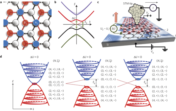
Although graphene has excellent electrical properties but since invent it faced one hindrance to using graphene in many applications has been the lack of a band-gap ( band-gap is an energy range in a solid where no electron states can exist ). That hindrance was partially overcome back in 2009 when a team working in the U.S. two layers graphene is different in that we can induce a large bandgap in it using an applied electric field. This cannot be done for single-layer graphene.
When layers of graphene are stacked on top of each other, they organize themselves in one of two main configurations – known as “Bernal-type” and “disoriented”. Bernal stacking occurs when the A-sublattice of one layer sits above the B-sublattice of the underlying layer. This “AB-stacked” configuration has the lowest possible energy, so under normal circumstances, this is the structure that multilayer graphene likes to adopt.
Since that time, researchers have been looking for ways to create such bilayer graphene in a way that could be commercialized. In this latest effort, the researchers report on a new technique they have developed that they claim produces the highest quality bilayer graphene yet.
Bilayer graphene has new tech to produce it high quality
How new tech work :
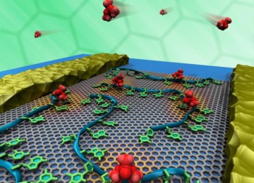
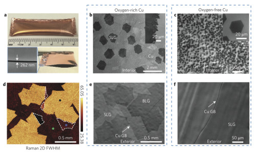
The new tech developed by the team results in just such a configuration in the chemical vapour deposition (CVD) chamber used to grow their graphene, it involves allowing a small amount of oxygen(parts per million concentrations) to enter a vapor deposition chamber where the graphene is being grown—the oxygen combines with a copper foil substrate causing a disassociation between methane molecules, releasing carbon atoms which then diffuse through the foil causing the second layer of graphene to form.
The team reports that the electrical properties of the material produced has similar electrical properties to that of exfoliated natural graphite (the substance found in pencil lead and which is just a few microns in size) comparable to graphene produced from graphite, and it has a band gap of approximately 125meV and it has a charge mobility of 60000 cm2V–1S–1 and a bandgap that can be tuned from 40 meV up to 100 meV. “To our knowledge, this is the first time that CVD-grown large-area AB-stacked bilayer graphene samples have been made with such high quality, which the team acknowledges is not high enough for making transistors but, they note it would likely work very well in optical applications such as for creating tunable photo-emitters and/or detectors. Explore further: Layering technique allows for creating graphene fiber that maintains conductivity and strength More information: Yufeng Hao et al. Oxygen-activated growth and bandgap tunability of large single-crystal bilayer graphene.