


New tech makes cheap graphene 100 times less previous methods
New tech makes cheap graphene 100 times less previous methods
Since discovered graphene in 2004 it has main disadvantage it’s high-cost product it in first days very small piece size as human hair cost about 1000$ but after that cost of product graphene became less and less but still very expensive ….. But now researchers at the University of Glasgow in Scotland have found a way to produce large sheets of high-quality graphene 100 times more cheaply than ever before.
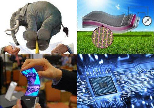
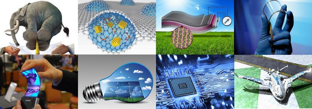
Graphene super strong material the miracle material can be used in almost anything and a lot of industries looking forward to using it ,Graphene is the world’s thinnest material at just a single atom thick, or one-million times thinner than a human hair, but is 200 times stronger than steel and conducts heat and electricity better than copper and it’s flexible, light and able to conduct heat and electricity better than most other materials out there, and have high-tech uses from integrated circuits, bendable mobile phone screens to prosthetic skin able to provide sensation. In fact, the only reason it hasn’t already revolutionised our energy, medical, and manufacturing industries are that it’s remained prohibitively expensive.
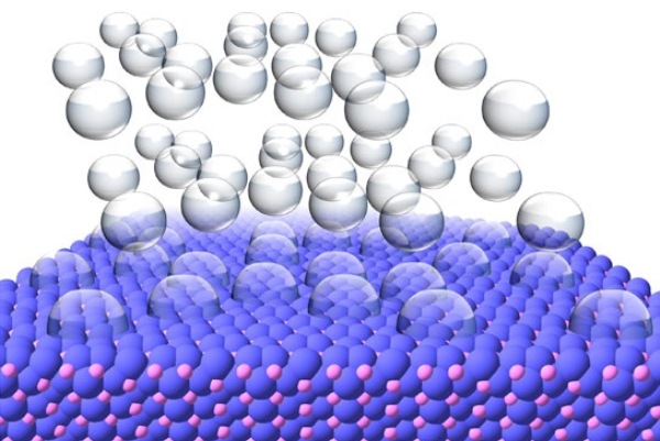
Currently, the most common method of making graphene is known as chemical vapour deposition, which is where gaseous reactants are turned into a film of graphene on a special surface known as the substrate.
Glasgow University’s research has discovered a way to produce large sheets of graphene with the same type of cheap copper used to manufacture lithium-ion batteries found in household appliances.
Dr Ravinder Dahiya, who led the university team working on the research, said: “The commercially-available copper we used in our process retails for around one dollar per square metre, compared to around $115 for a similar amount of the copper currently used in graphene production.
“This more expensive form of copper often required preparation before it can be used, adding further to the cost of the process.
“Our process produces high-quality graphene at low cost, taking us one step closer to creating affordable new electronic devices with a wide range of applications, from the smart cities of the future to mobile healthcare.”
Graphene is usually produced by a process known as Chemical Vapour Deposition, or CVD, which turns gaseous reactants into a film of graphene on a special surface known as a substrate.
The new technique will make it feasible for scientists to finally start using graphene in new innovations such as high-tech filters and materials, as well as medical devices.
“Much of my own research is in the field of synthetic skin. Graphene could help provide an ultra-flexible, conductive surface which could provide people with prosthetics capable of providing sensation in a way that is impossible for even the most advanced prosthetics today,” said Dahiya. “It’s a very exciting discovery and we’re keen to continue our research.”
Steps to graphene flakes had grown in copper foil , main tech to produce cheap graphene
New tech makes cheap graphene in details:
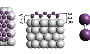
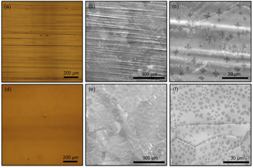
The surface quality of the Cu foils and the transfer process greatly influence the performance and reliability of graphene-based devices. Previous works have showed that the morphology of the Cu surface is one of the key parameters to have better quality graphene films. To achieve the continuous and high-quality graphene film over a large area; impurities, defects, grain boundaries and other surface features that can serve as a nucleation seed should be carefully engineered. To that end, a variety of techniques to smoothen the Cu surfaces has been reported. For example, Luo et al. used the standard electropolishing technique to smoothen the Cu surfaces. Their Raman investigation implied better quality graphene with higher surface coverage compared to the unpolished Cu samples. The similar electrochemical polishing technique was used in the work by Yan. et al. Together with the high-pressure annealing, they produced hexagonal single crystal graphene domains nearly 2 mm in size. Alternatively, melted Cu surfaces were also used to form single crystal hexagonal graphene flakes in previous works. It has been known that the quality of the Cu surface directly affects the charge carrier transport properties of the resulting graphene layer. Orfeo et al demonstrated the hole mobility of the graphene grown on the hetero-epitaxial Cu film is nearly 10 times greater than that of the graphene grown on the standard Cu foil by chemical vapor deposition. Above technologies including Cu polishing and deposition techniques add extra cost and time consuming chemical process steps which are not effective in the case of large-area synthesis of graphene.
The commercially available ultra-smooth Cu foils (which are generally used in Lithium-ion batteries) can help to open new avenues for large area device applications with the improved quality of the graphene films. We studied the synthesis of graphene on commercially available smooth Cu foils and we provided a detailed comparison between the graphene synthesized on ultra-smooth Cu foils and the one synthesized on the standard Cu foils in terms of structural, electrical and optical properties. We observed a stark improvement in the electrical performance of the transistors realized on our graphene films. Then, to demonstrate the advantage of high-quality graphene films from ultra-smooth Cu foils, we fabricated 400 cm2 flexible graphene electrodes and enlarged 160 times the previously reported (2.5 cm2) supercapacitor structure. To show the promises of our graphene films in electro-optic devices, we tested and compared the effects of graphene quality in large area supercapacitors. We anticipate that usage of commercially available ultra-smooth Cu foils for large area graphene growth would lead to higher performance devices especially for optical and electronic applications where low device variations are desired.