


Researchers enhance graphene photodetector by shaping it like snowflake
Researchers enhance graphene photodetector by shaping it like snowflake
Thanks to a novel gold fractal metasurface design, an international team of scientists from Purdue University and the Technical University of Denmark has managed to tune graphene’s natural wideband optical absorption by over an order of magnitude.
Published in Nano Letters, their article “Enhanced Graphene Photodetector with Fractal Metasurface” describes how the naturally poor photoabsorption of graphene (merely 2.3% of incident light) can be largely enhanced thanks to the metasurface’s role in facilitating the generation of electron hole pairs.
The meaning of fractal:
A fractal is a mathematical set that exhibits a repeating pattern displayed at every scale. It is also known as expanding symmetry or evolving symmetry. If the replication is exactly the same at every scale, it is called a self-similar pattern like in recursion but in different sizes. An example of this is the Menger Sponge.
Metasurface or an electromagnetic metasurface refers to a kind of artificial sheet material with sub-wavelength thickness and electromagnetic properties on demand. As shown in the review article given by Capasso et al., Metasurfaces could be either structured or not structured with subwavelength-scaled patterns in the horizontal dimensions.
The new approach beats other plasmonic nanostructure-based solutions which tend to be narrowband and polarization dependent, write the researchers, noting that their proposed gold fractal metasurface design has a relatively flat optical absorption in the visible part of the spectrum and is polarization insensitive.
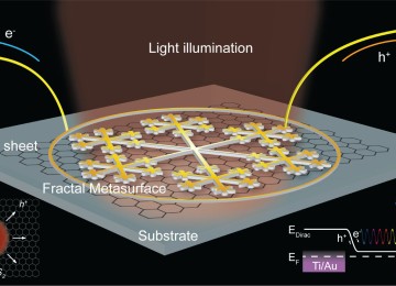
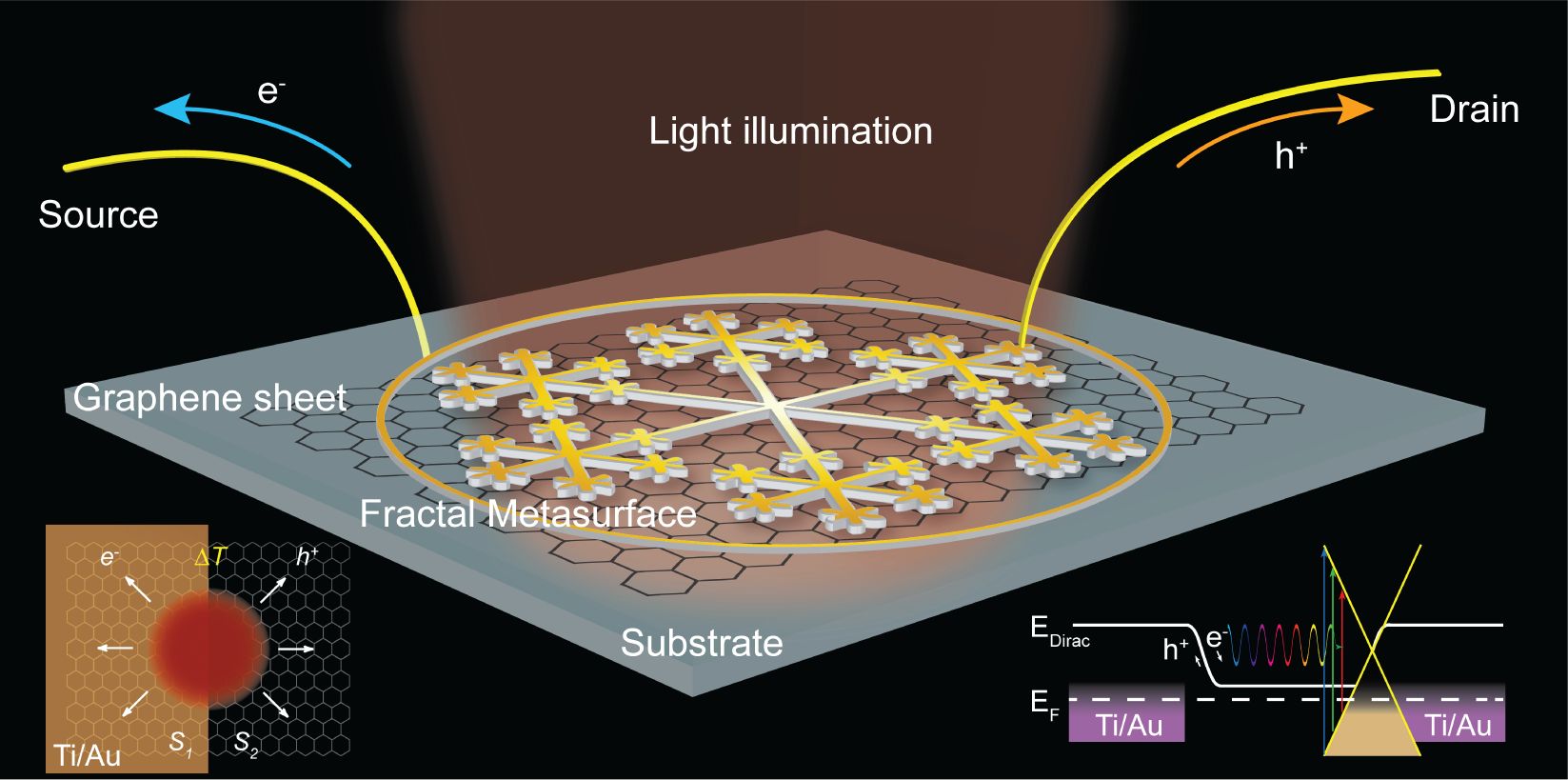
The metasurface consists of 40nm thick and wide gold lines patterned into a densified fractal snowflake geometry through electron beam lithography, out of a Ti (3nm)/Au (40nm) metallization layer.
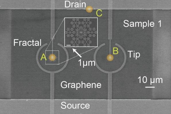
About 10μm in diameter, the tree-like structure incorporated six new branches spreading out from each new root points to four levels, and an additional three-level fractal structure densifying the original fractal concentrically. In their experiment, the fractal metasurface was connected to the drain of a graphene field effect transistor (with a graphene layer grown on a highly p-doped silicon substrate), circled out by a circular gold pattern extending out from the source.
For reference, the researchers also fabricated a tip-and-ring structure (without fractal metasurface) in parallel to the fractal metasurface-enhanced FET.
In agreement with their numerical simulations, they observed that when visible light hits the fractal metasurface, it excites plasmon oscillation in the gold fractal structure, which in turn confines and enhances the electric field of the incident electromagnetic wave within nanometers of the structure. This, they write, contributes to an extensive electron−hole pair generation and elevates the electron temperature through electron−electron interactions in graphene.
The generated carriers are then spatially separated/driven via the built-in electric field (PV) and thermoelectric power differential (PTE) at the gold−graphene interface, giving rise to a detectable photovoltage.
Using lasers as a light source focused on the snowflake electrode, they measured the photovoltaic output at different wavelengths, zero gate voltage and source−drain bias. The gold snowflake electrode yielded 10 to 16 better performance than the reference tip-and-ring electrodes.
The researchers also observed that the amplitude of the photovoltage increased monotonically with increasing source−drain bias and the photovoltage could be tuned up to three times of that at zero bias.
Although all the experiments were done with one particular snowflake design, the researchers note that the simple and inward scalability of fractal metasurfaces makes them well suited for further densification as well as easily adapted to various geometries (the overall coverage area is unchanged with increasing fractal levels, thus the design can be further optimized and still well contained).
They also suggest that such fractal metasurfaces could also be integrated with photovoltaic or photo thermoelectric devices made of other materials than graphene.