


Scientists gets world-first images of electric currents in graphene
Scientists gets world-first images of electric currents in graphene
Researchers at the University of Melbourne are the first in the world to image how electrons move in two-dimensional graphene, a boost to the development of next-generation electronics.
Capable of imaging the behavior of moving electrons in structures only one atom in thickness, the new technique overcomes significant limitations with existing methods for understanding electric currents in devices based on ultra-thin materials.
“Next-generation electronic devices based on ultra-thin materials, including quantum computers, will be especially vulnerable to contain minute cracks and defects that disrupt the current flow,” said Professor Lloyd Hollenberg, Deputy Director of the Centre for Quantum Computation and Communication Technology (CQC2T) and Thomas Baker Chair at the University of Melbourne.
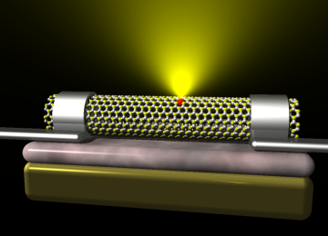
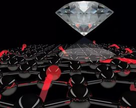
A team led by Hollenberg used a special quantum probe based on an atomic-sized ‘color center’ found only in diamonds to image the flow of electric currents in graphene. The technique could be used to understand electron behavior in a variety of new technologies.
“The ability to see how electric currents are affected by these imperfections will allow researchers to improve the reliability and performance of existing and emerging technologies. We are very excited by this result, which enables us to reveal the microscopic behavior of current in quantum computing devices, graphene, and other 2D materials,” he said.
“Researchers at CQC2T have made great progress in the atomic-scale fabrication of nanoelectronics in silicon for quantum computers. Like graphene sheets, these nanoelectronic structures are essentially one atom thick. The success of our new sensing technique means we have the potential to observe how electrons move in such structures and aid our future understanding of how quantum computers will operate.”
In addition to understanding nanoelectronics that control quantum computers, the technique could be used with 2D materials to develop next generation electronics, energy storage (batteries), flexible displays and biochemical sensors.
“Our technique is powerful yet relatively simple to implement, which means it could be adopted by researchers and engineers from a wide range of disciplines,” said lead author Dr. Jean-Philippe Tetienne from CQC2T at the University of Melbourne.
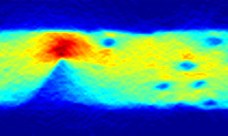
An image of the current flow in graphene, obtained using a diamond quantum sensor
“Using the magnetic field of moving electrons is an old idea in physics, but this is a novel implementation at the micro-scale with 21st Century applications.”
The work was a collaboration between diamond-based quantum sensing and graphene researchers. Their complementary expertise was crucial to overcoming technical issues with combining diamond and graphene.
“No one has been able to see what is happening with electric currents in graphene before,” said Nikolai Dontschuk, a graphene researcher at the University of Melbourne School of Physics.
“Building a device that combined graphene with the extremely sensitive nitrogen-vacancy color center in diamond was challenging, but an important advantage of our approach is that it’s non-invasive and robust – we don’t disrupt the current by sensing it in this way,” he said.
Tetienne explained how the team was able to use the diamond to successfully image the current.
“Our method is to shine a green laser on the diamond, and see red light arising from the color center’s response to an electron’s magnetic field,” he said.
“By analyzing the intensity of the red light, we determine the magnetic field created by the electric current and are able to image it, and literally see the effect of material imperfections.”